UNISOC introduces UniSwap Ultra Engine for managing flash memory smartphone RAM
Read more
Pandaily
pandaily.com

UNISOC introduces UniSwap Ultra Engine for managing flash memory smartphone RAM

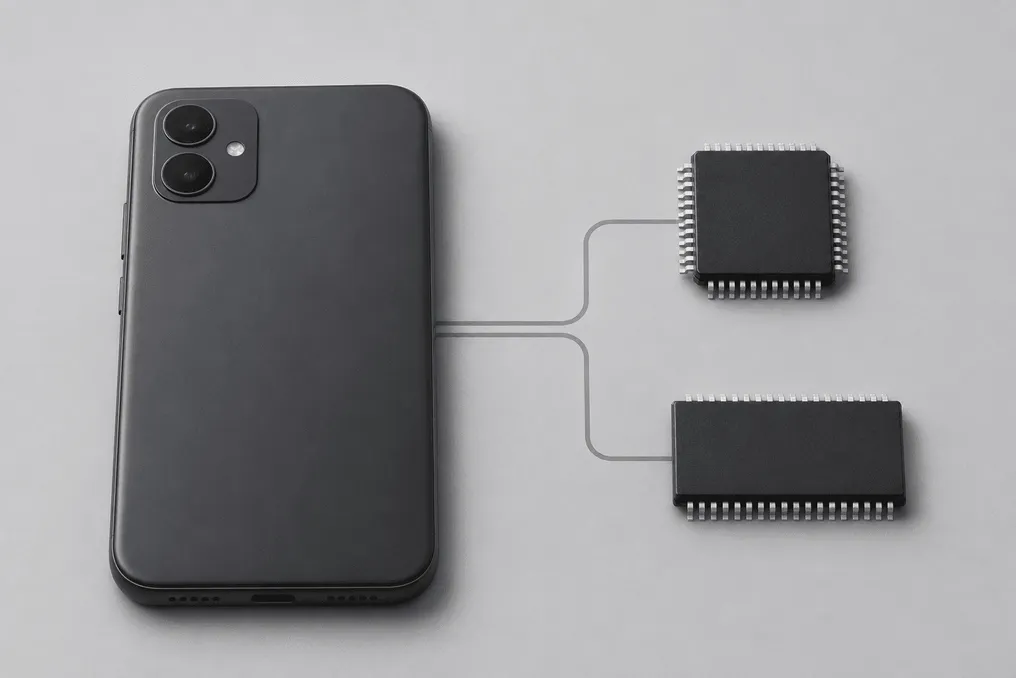
UNISOC has announced the UniSwap Ultra Engine—a memory management system for smartphones that combines chip-level scheduling, compressed memory, and a flash memory-based paging mechanism. This technology was presented on November 20th, with Chinese reports detailing its architecture and laboratory results the following day.

The mechanism utilizes UFS storage to expand the amount of memory available to applications when physical Random Access Memory (RAM) is limited. It is important to note that this is a virtual memory technique, not an installation of additional DRAM. For example, a smartphone with 4GB of physical RAM will not automatically become a device with 6GB of physical RAM just by using part of the storage for paging.

According to UNISOC statements, a 4GB smartphone using this scheme can achieve daily smoothness comparable to a traditional 6GB model. Furthermore, the company reports a 20% reduction in system latency and a 20% improvement in background application retention. These metrics are directly attributed to UNISOC's laboratory tests, not independent device testing.

Engine Structure and Operating Principles

The system is described in three levels. At the System-on-Chip (SoC) level, CPU and DDR Quality of Service controllers regulate bandwidth, frequency, and access time in response to workload changes. To reduce latency when moving data between memory and storage, UFS controller optimizations, physical interface optimization, priority access, and data prefetching are used.

The software level is responsible for compressing memory used by background applications and dynamically distributing this compressed volume between ZRAM and UFS. It also manages application lifecycles and memory freeing processes. The goal is to minimize the need for complete application restarts when users switch between messengers, videos, games, and other tasks.

The third level involves collaboration with storage manufacturers regarding flash memory characteristics, firmware, and file system coordination. UNISOC claims that its custom-developed UFS solutions account for endurance and latency requirements during repeated paging traffic. However, the announcement does not include independent durability measurements confirming similar benefits for all types of storage.

These statements relate to coordinating existing memory and storage resources, not presenting a new device or proving that flash memory possesses physical properties similar to DRAM. Actual results will depend on the type of application workload, compression behavior, storage hardware, and device integration. The announcement does not provide a full list of phones that will use this technology, nor does it offer a reproducible protocol for third-party comparison. The specific contribution lies in the described approach to chip and software integration; percentage improvements and experience remain vendor-claimed results.


Similar stories

Tencent releases Hy4 flash model weights for download in three variants
Read more
pandaily.com

Tencent releases Hy4 flash model weights for download in three variants

Tencent has published the downloadable weights for the Hy4 flash model following the announcement of its API on November 16th. This was reported by IT Home on November 18th. This update provides deployable checkpoints, rather than a re-presentation of the API specifications and pricing previously covered by Pandaily.

The official Tencent model page lists three versions: Hy4 flash, which is an instruction-tuned model; Hy4 flash-FP8, its instruction-tuned quantized version; and Hy4 flash-base, a pre-trained base model. The base checkpoint is intended for further training, not to replace the chat-ready variants.

Pandaily verified all three official repositories on Hugging Face. The weight index files referenced available shard lists, and anonymous byte range requests returned weight file data for each version. These checks confirm the availability for download but do not constitute full checkpoint downloads or successful output tests.

The standard checkpoint contains approximately 440.5 GB of tensor data, while the FP8 version is about 287.1 GB. These sizes refer to the weight data, not the minimum GPU memory requirements. Quantization reduces storage size but does not turn the release into a model suitable for small consumer devices.

Deployment documentation is an important part of this release. Tencent provides specialized vLLM and SGLang container images, including examples of eight-way tensor parallelism. Instructions for Transformers point to requesting model support rather than assuming that the standard released package already supports this architecture.

The vLLM recipe also requires host RAM, as Engram tables are defaulted to be offloaded to CPU memory. The initial configuration uses a context size of 8192 tokens; the model's claimed capacity of 1 million tokens does not guarantee that every hardware configuration can handle such length. The published memory hints are estimates, not measured minimum requirements.

The checkpoints use the Tencent Hy 1.0 license, which explicitly states that it is not Apache 2.0, despite being derived from it. Section 10 requires a separate written license for Model-as-a-Service operators whose cumulative global revenue exceeds $50 million over a consecutive 12-month period, or for using the model in a product or service with more than 100 million monthly active users. A narrowly defined exception applies to internal use when the model and its outputs are not provided to third parties.

Thus, this release is best described as open in terms of weights according to Tencent's stated terms, rather than as unrestricted open source. Tencent reports that the release of the larger Hy4 model weights is still in preparation.

D-Robotics and Infinigence AI integrate open robotics tools into Sunrise chips
Read more
pandaily.com

D-Robotics and Infinigence AI integrate open robotics tools into Sunrise chips

D-Robotics and Infinigence AI announced an agreement under which a set of open-source tools for embodied artificial intelligence will be integrated with D-Robotics' Sunrise chips and its RoboGo software platform. This was announced by both companies on November 13.

It is reported that some components are already working together, allowing developers to complete the full development cycle: training models, controlling devices, launching agents, and deploying them on robot hardware within a unified workflow.

This open-source toolset covers four stages of robot development. It was jointly developed by Tsinghua University and Infinigence AI.

D-Robotics is responsible for providing the hardware and platform. Its Sunrise chips provide access to devices and on-board operation execution, while RoboGo handles environment management, task planning, and execution monitoring.

According to company statements, the integration has already demonstrated results: developers can select a training environment in RoboGo, remotely control and call peripheral equipment, and conduct model training, agent execution, and testing with feedback from the hardware all within one process.

This announcement expands upon previous work shown by both parties. Infinigence AI opened the source code for APXInf in September, using the optimized Pi0.5 model for NVIDIA Jetson Thor, and the S600 adaptation added a domestic robot chip to its target solutions. D-Robotics previously combined third-party robot models with Sunrise S600, including GigaBrain-0.7 from GigaAI.

Neither company has published performance metrics for the combined workflow nor stated when more Sunrise models will support APXInf.

Google launches TPU 8tx and TPU 8i Max for data protection and increased memory in AI
Read more
olhardigital.com.br

Google launches TPU 8tx and TPU 8i Max for data protection and increased memory in AI

Google has unveiled two new artificial intelligence (AI) chip systems, named TPU 8tx and TPU 8i Max, which represent an expansion of the eighth generation of its processors. One of these new devices was specifically designed to ensure data protection during processing, while the other was created to manage large volumes of information used by AI agents.

With these launches, the corporation now offers four eighth-generation TPU systems in a single year, each tailored to different demands for model training and execution. These devices complement the TPU 8t and TPU 8i, which were presented in April during the Google Cloud Next event.

The TPU 8t is focused on large-scale model training, and the TPU 8i is intended for tasks requiring agile responses. According to Google, these new chips provide up to 2.7 times more performance in training and offer 80% better cost-performance ratio in inference compared to the previous generation, respectively.

The TPU 8tx is aimed at companies and government agencies that need to handle confidential information without it being exposed during the computation process. Meanwhile, the TPU 8i Max was designed for applications that require the simultaneous analysis of vast amounts of data, such as AI agents examining extensive code or long video recordings.

The TPU 8tx integrates confidential computing functionalities directly into its hardware. This allows data and internal model information to remain secure even when being utilized by the system. This feature is suitable for organizations that handle private data or need to comply with very strict security standards.

This equipment uses the same processing technology as the TPU 8t but combines it with fifth-generation AMD EPYC processors and the Boardfly network. Google reported that this combination results in a response time up to half that of the TPU 8t, without causing a significant impact on performance.

The architecture also supports adapting AI models using private data, creating reduced versions from larger models, and training agents without the need to transfer information between different server sets.

The TPU 8i Max consolidates two TPU 8i chips into a single physical structure, giving it double the processing capacity and memory resources compared to the standard model. Furthermore, Google mentioned that this system concentrates twice as many processing components in the same rack space, allowing for greater computational capacity in data centers.

In addition to the hardware, the company introduced tools to assist developers. TorchTPU, released as open source, allows applications developed with PyTorch and Hugging Face models to run on TPUs without requiring code rewriting. Another innovation is TPU Sync, which improves communication between chips, servers, and storage systems, optimizing access to information that AI reuses when generating responses. Google stated that this can decrease the data transfer time and waiting time for the first word or part of a response by over 90%.

Finally, Cloud Pathways became generally accessible on Google Kubernetes Engine (GKE). This tool facilitates the coordination of multiple sets of TPU processors as if they were a single unit, simplifying the execution of tasks that require high processing capacity.

Google reported that about 100 customers already use its TPUs, covering AI laboratories, financial institutions, retailers, and universities. The company itself employs artificial intelligence tools, such as AlphaChip and Gemini, to accelerate the development of its own processors.

Popular