Huawei Confirms Use of In-House HiSilicon 1-Inch Sensor in XMAGE Z10 and Details Kirin 9050 Security
Read more
Pandaily
pandaily.com

Huawei Confirms Use of In-House HiSilicon 1-Inch Sensor in XMAGE Z10 and Details Kirin 9050 Security

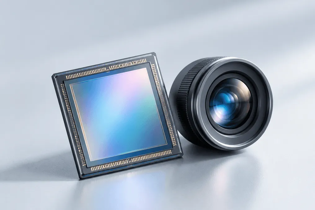
Huawei announced that the XMAGE Z10 camera module is equipped with an image sensor developed in-house by the HiSilicon chip design division. This information was presented during the Kirin 2026 media briefing, held at the company's research center in Lianqiu Lake, Shanghai, on October 13. At the event, Su Songyu, Head of Wireless Terminal Chip Product Management in Huawei's semiconductor business, provided more detailed information about the Kirin 9050 series beyond the previously shown architectural diagram.

According to a report by IT Home on site, the Kirin 9050 series is designed for close integration with the new generation of self-developed CMOS image sensors, fully customized optics, and a professional Image Signal Processor (ISP) for image processing. This allows Huawei to customize the entire chain independently, from the sensor and lens to the processing on the chip. Su stated that the XMAGE Z10 uses a 50-megapixel 1-inch RYYB sensor developed by HiSilicon. Previous coverage of this module mentioned the sensor's size and color filter but did not specify the developer.

The XMAGE Z10 was released on October 1 along with the Mate 90 series. It attaches via Huawei's HyperClick mount, available in H1 and H2 versions for the Mate 90 Pro Max and Mate 90 RS collector editions, supporting quick attachment without screws. The module features its own optical image stabilization system that works in conjunction with the Kirin chip, and it is priced at 5,999 yuan, or 19,499 yuan in the collector's bundle.

Regarding security, Huawei stated that the Kirin 9050 series is among the first mobile SoCs to undergo official testing for quantum attack resistance, including support for post-quantum cryptography. The company also named it the first SoC platform with chip-level protection: the mobile security processor interacts with a dedicated security chip to protect boot, data, privacy, and communications.

In terms of audio and video, the chip integrates heterogeneous DSP and NPU computing with low-latency FFTS scheduling and H.266 hardware video decoding. Huawei noted that this improves call clarity and sound processing, as well as making video playback smoother and more energy-efficient with weak network connections. However, Huawei did not disclose the name of the body that conducted the anti-quantum attack certification nor provide additional technical specifications for the new sensor.
Similar stories

Richard Yu states that more Huawei phones will receive LogicFolding chips as part of the Tau roadmap
Read more
pandaily.com

Richard Yu states that more Huawei phones will receive LogicFolding chips as part of the Tau roadmap

Richard Yu, CEO of Huawei and Chairman of its Consumer Business Group, announced at an international roundtable that Huawei's LogicFolding chips will not be limited to just a few flagship devices. He stated that more Huawei phones utilizing chips developed according to the Tau scaling law (τ) will be released.

The LogicFolding technology first appeared in Huawei phones with the Mate XT 2 tri-fold model, and Yu noted that it will gradually begin to be integrated into a wider range of the company's smartphones. However, he did not specify particular models or timelines for mass release.

The speed of this expansion, according to Yu, partially depends on production capacity. He expressed hope that China's semiconductor industry can increase its manufacturing capacity so that Huawei can create more advanced products for consumers both domestically and internationally.

Details of the Kirin 9050 Pro chip

At the same roundtable, Yu presented details of the Kirin 9050 Pro chip, which is used in the top-tier Mate 90 models. Huawei independently developed components such as the Balong modem, Image Signal Processor (ISP), Mobile Security Processor (MSP), Lingxi CPU, Maleoon GPU, and an NPU built on the Da Vinci architecture. He emphasized that the overall phone performance is 31% higher than the previous generation, and the in-house development ensured better energy efficiency and system performance despite limited access to advanced manufacturing processes.

Technology Development Roadmap

Comments on the expansion are accompanied by a long-term development plan. According to the trajectory of the Tau scaling law, Huawei chips in 2026 will reach a performance core frequency of 3.1 GHz, which is 12.7% higher than the 2.75 GHz of the Kirin 9030 Pro. Further plans include stable growth in frequency and transistor density, reaching over 400 million transistors per square millimeter and a clock frequency of 5.0 GHz by 2031.

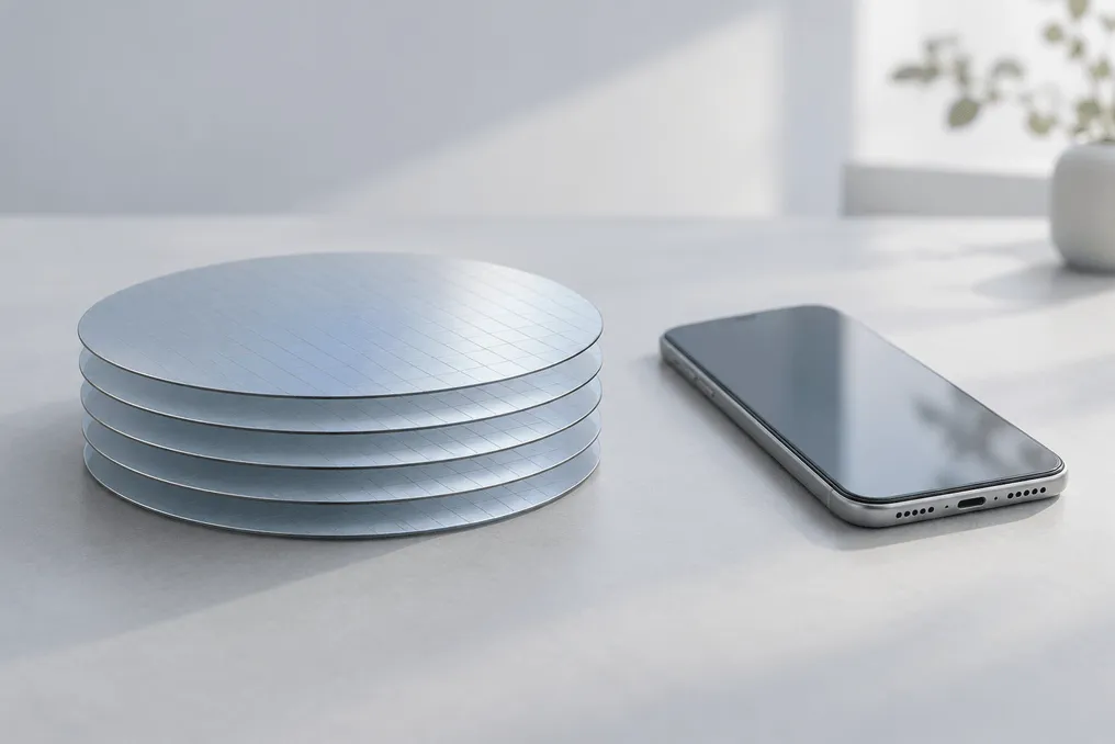
The LogicFolding technology works by vertically stacking logical layers of the chip and using dense inter-layer connections to shorten critical paths and reduce latency, instead of relying solely on reducing transistor size. Huawei has not yet specified which product lines will use this technology in the next phase, or whether mid-range phones will be included.

Popular