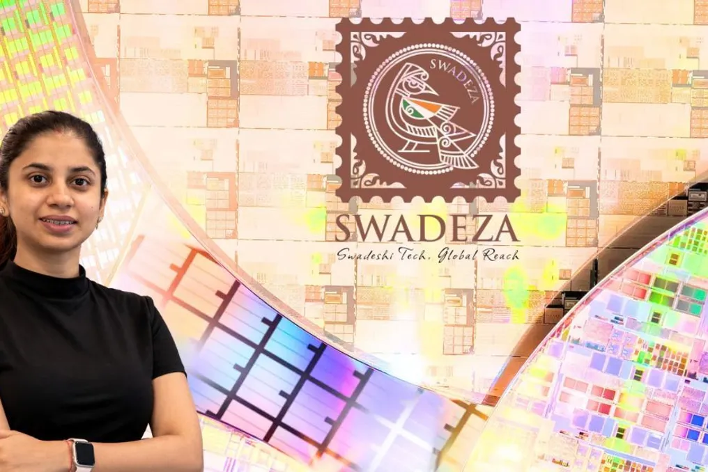
The question of what the concept of 'Made in India' might look like if globally significant technologies are created in regions rarely associated with deep technology has led to the creation of Swadeza. Today, Swadeza is developing from Bihar, with ambitions extending far beyond its geography. This also reflects a broader shift in India's technological landscape concerning the origin of the country's next generation of tech companies and who will create them.
Founder Shweta Suman followed a non-linear path: she studied in Oman, received an engineering degree at BIT Mesra, returned to Oman, and then moved back to Bihar after marriage. Instead of seeking opportunities elsewhere, she decided to build the company right here.
This choice is significant in the context of the state. Bihar is often discussed in terms of migration, where talent and opportunities leave the region. Suman's journey goes in the opposite direction: returning, establishing a tech company, integrating into India's startup ecosystem, and ultimately presenting Swadeza at one of the country's most prominent semiconductor industry conferences.
Swadeza operates in semiconductor technology, IT consulting and development, as well as 360-degree digital marketing. Its deep technology work is increasingly focused on AI-oriented semiconductor design. In software, the company creates platforms for government and public sector entities. The company positions itself as a women-led enterprise, stating that its engineers have an average of 11 years of experience in fabless semiconductors, consumer platforms, and government deployments.
Furthermore, Swadeza developed an AI-based automated verification system for government recruitment in the Bihar Government, which, according to the company, reduced processing times from several months to several weeks. Before a chip is sent for production, engineers must prove that the design functions exactly as specified. This verification is one of the most labor-intensive stages of chip development, and errors found after the tape-out stage are costly.
Swadeza argues that general-purpose AI assistants struggle to operate at this scale. As the design grows, the assistant's prompt becomes filled with unrelated and contradictory fragments, leading to a decrease in answer quality. Instead, its semiconductor platform, FORGE, keeps the chip in a cited map, passes only the information relevant to the specific query to the language model, and converts the acquired knowledge into deterministic models, ensuring that each run is faster and cheaper than the previous one.
FORGE is designed to implement AI-driven workflows throughout the entire chip lifecycle: from verification and physical design to post-silicon validation and standard cells. The DV-FORGE system handles verification; it reads the chip's reference manual into a map and generates a verification plan, coverage model, and UVM test environment based on it. The company reports that DV-FORGE was used for the OpenTitan class SoC, successfully completing the verification of the OpenTitan Earlgrey root-of-trust chip in 30 days and finding seven errors across approximately 40 IP blocks and 2581 registers. Its derivative, Darjeeling, was verified in 21 days, with most of the time spent on regression testing. Swadeza also claims to use 80% fewer tokens than an AI assistant and has applied this pipeline to reference manuals from NXP, STMicroelectronics, Renesas, and Infineon.
PD-FORGE is being developed to close physical design, allowing tracking of violations during sign-off back to the stage that caused them. It links reports from all stages, runs, and tools to the same nets, covering 26 backends from Synopsys, Cadence, Siemens, and open sources, and is currently undergoing closed testing before production release in Q4 2026. PS-FORGE, intended for post-silicon validation and debugging, and SC-FORGE, which aims to create provably optimal standard cells, are still under development.
FORGE is deployed locally. In an industry where chip designs are among the most confidential corporate intellectual assets, storing data in client environments eliminates a major hurdle for implementing AI-based tools. Swadeza states that it collaborates with professors from BIT Patna and with Signitude, a fabless semiconductor company.
At SEMICON India 2026, Swadeza presented its semiconductor technologies alongside some of the industry's most recognized names. It was also the first public demonstration of FORGE at Startup Booth 6. The fifth edition of SEMICON India took place from September 17 to 19 under the theme 'From Silicon to Systems: Building the Ecosystem'. It occurred two months after the approval of Semicon 2.0 by the Cabinet—India's second phase of the ₹127,500 crore chip mission.
Following this, Swadeza was featured in Forbes India's photo report of the event, in the same visual overview as IBM and Tata Electronics. For a company that chose to build from Bihar, this moment held significance far beyond publicity. It placed a product made in Bihar on par with global leaders in semiconductors.
Bihar itself is actively promoting itself in this sector. The state cabinet approved its Semiconductor Policy 2026 earlier this year, aiming to attract manufacturing capacity, display fabs, and chip design facilities. A Bihar Semiconductor Mission has also been established to oversee implementation. Much of this policy focuses on investment in manufacturing. Swadeza represents a different kind of participation: locally created design tools intended for chip development teams anywhere in the world.
Swadeza's broader vision is to build from India for the global market. The immediate tests are clear: transitioning PD-FORGE into production operation and converting conversations from SEMICON into paid local implementations with chip development teams. If successful, Swadeza will prove that India's deep tech companies do not have to start in traditional hubs, and that the next wave of creators can emerge from places the ecosystem overlooked.