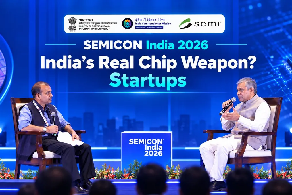
Support for microchip design startups in India will receive a significant boost following the Union government's approval of the Semicon 2.0 program, which provides for more than doubling state support for this segment. The Minister of Electronics and Information Technology, Ashwini Vaishnaw, announced this during a fireside chat at the SEMICON India 2026 event on September 18, 2026.
His comments, made as the second phase of India's semiconductor incentives was formulated, place the country's ambitions in the chip domain at the center, encompassing both deep technology developers and SME manufacturing bases, alongside large investments in fabrication plants.
Ashwini Vaishnaw noted that India's pursuit in semiconductors began six years ago under Semicon 1.0. He emphasized that previous attempts, spanning nearly six decades, had repeatedly failed due to inconsistent policies and short-sightedness.
This time, the government has developed a program based on a twenty-year roadmap and a phased approach. This approach started with Assembly, Testing, Marking, and Packaging (ATMP) units and the first fabrication plant for a relatively less complex, high-throughput chip segment—on a node from 28 to 90 nanometers, which, according to the minister, accounts for about 70% of the global chip volume. It is worth noting that Semicon 1.0, planned as a six-year project, was completed in only four years, allowing for the creation of a foundation for its successor.
Semicon 2.0, approved with allocations of ₹1.275 billion, is based on six key areas: design, materials and equipment, additional fabs, expansion of ATMP capacities, research and development, and talent. Vaishnaw pointed out that chip design proved to be the most startup-dense area among these directions.
Under Semicon 1.0, the government eliminated, according to Vaishnaw, the biggest hurdle for young design companies—the high cost of licensing Electronic Design Automation (EDA) tools from suppliers like Cadence, Synopsys, and Siemens. Instead of funding individual licenses, access to these tools was organized jointly through the Centre for Development of Advanced Computing (C-DAC). As a result of this step, over 105 startups became chip designers, with 20 of them attracting venture capital, estimated at around ₹800 billion, according to early government data.
Building on this foundation, Semicon 2.0 aims to support at least 200 companies engaged in deep chip design, which Vaishnaw called a potential turning point for Indian intellectual property.
Beyond chip design, Vaishnaw highlighted the program's positive impact on small and medium Indian manufacturers. Quoting an industry leader he met at the event but not naming the company, he reported that the company had already begun exporting components worth about ₹2,000 billion from India, with almost 90% of this component ecosystem sourced from SMEs.
He added that the precision manufacturing capabilities established around electronics assembly are now being utilized across various sectors, including mobile phone production, aerospace components for companies like Airbus, and defense industries, in addition to semiconductors. One executive Vaishnaw spoke with noted that his company's board of directors informed him there was no actual limit on investment in India, provided execution timelines were met, which he felt indicated investor confidence in the program.
To support this transition, the government is implementing a multi-tiered training system, starting with a Level 1 course lasting 240 hours, designed to prepare a student immediately after high school with skills comparable to a college engineering graduate at subsequent levels. A specialized Institute of Precision Manufacturing is soon planned, followed by similar institutes.
Regarding the total number of specialists, Vaishnaw stated that India has set a goal to train 85,000 semiconductor design engineers over ten years and has already trained about 70,000 in the first four years. He clarified that other recent government statements indicate achieving the full target of 85,000, so the exact current number may vary depending on the date of the last update. Furthermore, he noted that the target of one hundred thousand cleanroom technicians under Semicon 2.0 would likely require an increase given industry demand.
One detail from the conversation helps explain the rapid growth of chip design startups in India. EDA tools are specialized software used for chip layout and modeling before production. Licenses from suppliers such as Cadence and Synopsys can exceed a startup's early-stage annual budget.
Instead of subsidizing individual purchases, the government viewed access to EDA as shared infrastructure through C-DAC, allowing startups to design chips without bearing these costs independently. Vaishnaw suggested that this approach influenced the development of India's chip design ecosystem more than direct grants, as it lowered the barrier to even attempting to design a chip. However, it remains an open question whether this model will hold up when scaled to a cohort nearly double the initial one under Semicon 2.0.
In conclusion, Vaishnaw mentioned that India's first fab, the Tata Electronics-PSMC facility in Dholera, is expected to reach first silicon in 2028. He noted that the spot reserved for this silicon in his office is currently empty, serving as a reminder of how much of the Semicon 2.0 promises still needs to be realized. For chip design startups and SMEs supporting this ecosystem, the upcoming phase will test how well policy based on shared infrastructure and phased training can scale beyond the initial group.