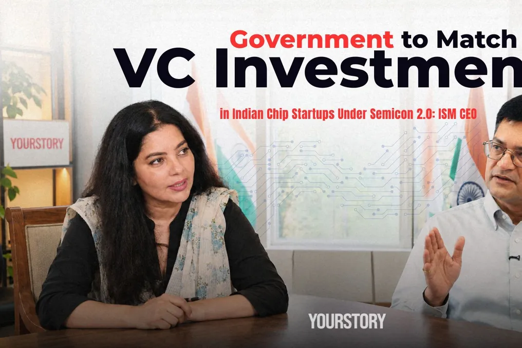
Job opportunities in India's semiconductor industry are available to a wide range of specialists, not just graduates from leading universities
Read more
YourStory [india, en]
yourstory.com

Job opportunities in India's semiconductor industry are available to a wide range of specialists, not just graduates from leading universities

Women working on chip packaging lines at the CG Power plant in Sanand, Gujarat, come from regions such as Jharkhand, Madhya Pradesh, Bihar, Odisha, and the Northeast. They had only ordinary education and did not expect to work in the semiconductor industry. After training in Malaysia, they now explain the chip packaging process 'like confident engineers,' according to Amitesh Kumar Singh, Additional Secretary of MeitY and CEO of India Semiconductor Mission. He told Shraddha Sharma, founder and CEO of YourStory and The Bharat Project, ahead of the Semicon India 2026 event that this is the essence: jobs in the semiconductor sector in India are open to students of any discipline, not just those who have achieved high scores in entrance exams.

Singh noted that semiconductors may initially seem like a very complex field. The example from Sanand serves as an answer to this concern. This initiative was announced against the backdrop of the launch of Semicon 2.0, the second phase of the mission, which was approved on August 31, 2026, with a budget of ₹1,275 crore. This phase complements the incentives for fabrication and packaging in the first phase by adding areas dedicated to talent and research and development.

Currently, twelve manufacturing facilities have been approved, three of which—Micron, Kaynes, and CG Semi in Sanand—are already operating commercially. In response to Shraddha's question, which a student from Patna, Indore, or Kochi might ask, about whether this industry is exclusively an IIT startup club, Singh replied that the industry has ceased to be elite, let alone purely electronic. A factory requires not only engineers but also operators and R&D specialists. Chemical, gas, and materials needs require chemists and material scientists. Building factories is complex enough to require serious civil engineers. Robotics and physical AI in manufacturing require mechanical engineers. Even chip design, which was previously purely electronic, now includes expertise in thermal engineering and materials. According to him, 'every discipline has a connection to semiconductors.'

The talent pillar under Semicon 2.0 aims to create training programs that allow a graduate from a chemical or mechanical faculty to transition into a role in the semiconductor industry. The industry has a multiplier of about 5.7, meaning one factory creates significantly more subsequent jobs than at the facility itself. Singh emphasized that women already constitute more than half of the workforce in India's electronics industry, reaching 70% in some places and entire shifts in some plants, and he expects semiconductor enterprises to follow this example. Semicon India 2026 has scheduled a special session dedicated to women in this industry, featuring senior leaders from Renesas, Applied Materials, Teradyne, and Micron.

For those interested in design, the path is no longer limited to a few educational institutions. The Chips to Startup program provides colleges with free access to automated electronic design (EDA) tools, software necessary for chip development, which small teams would otherwise not have access to. According to PIB, over 300 academic institutions gained access in January 2026, and Singh noted that the reach extends to all states, including smaller colleges. Designs created by students that reach the manufacturing stage are produced in the Semiconductor Laboratory in Mohali or elsewhere, then packaged and returned. He stated that 'a student who goes through the full cycle leaves college as a confident design engineer and can start their own startup.'

Such startups receive seed grants and EDA tools under the Design Linked Incentive scheme. Under Semicon 2.0, the government will match, acting as an investor on the same terms, any attracted venture capital after the initial stage. Singh suggested that a student who is not yet ready to start alone can join a startup founded by a senior specialist, gain experience over three to four years, and then establish their own business.

The top of the career ladder is also filled from the reverse direction. Thanks to Design Linked Incentive, many Indians with 25 to 30 years of chip design experience, who worked in Silicon Valley and beyond, now want to return home and start their own ventures. Indians abroad are also joining companies like Tata, CG Power, and Micron, as these companies are creating R&D teams in India. A chip design company can have between 50 and 200 people, and 'if it becomes large, it turns into Qualcomm, which hires 20,000 engineers in India.' He listed all major multinational corporations such as Intel, AMD, Qualcomm, Broadcom, NVIDIA, NXP, and Infineon, noting that each has one of the largest design centers here, and 20% of global design engineers are already Indian. Thanks to the specialized R&D focus under Semicon 2.0, he concluded that 'young people focused on R&D do not need to go abroad.'

The nearest opportunity is presented by the workforce development pavilion at Semicon India 2026, which will take place from September 17 to 19, 2026, in Yashoboomi in Dwarka, New Delhi. It will feature mentorship for students, training on the full factory production process, a one-day session with experts from Singapore on September 18, and company-funded hackathons. Singh advised: 'This opportunity is available, and no one should miss it.' The women from Sanand did not have such a pavilion, but the next group will.

Similar stories

India Semiconductor Industry Head Explains Microchip Creation Process from Raw Materials to Finished Chip
Read more
yourstory.com

India Semiconductor Industry Head Explains Microchip Creation Process from Raw Materials to Finished Chip

Every user of a phone, laptop, or UPI application in India relies on semiconductors, yet most people have never seen the chips themselves. In connection with the opening of Semicon India 2026 in New Delhi on September 17, 2026, Amitesh Kumar Sinha, Additional Secretary of MeitY and CEO of India Semiconductor Mission, held a discussion with Shraddha Sharma, founder and CEO of YourStory and The Bharat Project. He explained in detail how a semiconductor chip is created using a simple analogy—the chip is like a house.

Sinha compared the chip creation process to building a house: first comes the design, then the construction, and finally, doors and windows are installed to make the object functional. This demonstration is important because it explains the basis for the government allocating funds amounting to 127,500 crore rupees for the second phase of the mission, which was announced on August 31, 2026.

Any element that conducts electricity and interacts with the user logically—from a Google search query to AI servers, defense equipment, and home appliances—functions thanks to chips. Like a multi-story house, a chip is built in layers. If a house is designed using CAD tools, a chip is developed using EDA tools, or Electronic Design Automation. The complexity of such a design is so high that Sinha ranks it among the world's most complex technologies.

The majority of financial investment goes into the design stage. Approximately half the cost of the entire semiconductor chain is attributed to design. The cost of developing a single chip can range from a modest 25 crore to 35 crore rupees, while the most complex components can cost from 1,000 crore to 2,000 crore rupees. This is why startups were given free access to EDA tools in the first phase of the mission, and state co-investment is planned for the second phase after a venture fund supports the design startup.

After the design is completed on computers, it is transferred to the fabrication plant (fab). Engineers at this plant require the design in their own machine language, so the development team works with the foundry's Process Design Kit (PDK), which Sinha describes as the foundry's own set of EDA tools. After agreement and creation of the design file, it is sent for production. Sinha compares the factory to a kitchen: 'Give it a recipe, and it will produce the product.'

Chips are not produced one by one. They are manufactured on a large circular crystal, which Sinha equates to the initial structure of a building: columns, pillars, and walls before final finishing. Wafers come in sizes of 12, 8, 6, and 4 inches. For silicon logic and memory fabs, 12 inches is the standard, whereas for connections based on advanced semiconductors like silicon carbide and gallium nitride, 8 and 6-inch wafers are more commonly used today.

The raw material is the wafer itself. Silicon is purified from quartz sand into an ultra-pure crystal, which is grown as a cylindrical ingot and then sliced into thin discs that arrive at the factory with mirror polishing. Inside the factory, a multi-stage process involving hundreds of steps takes place: layers of material are deposited onto the wafer, patterns are printed on them using light in a process called lithography, and unnecessary material is etched away. This cycle repeats layer by layer over weeks until the circuit is complete.

One can imagine many houses on one plot of land. One crystal contains many identical chips, and the process called dicing separates them. Sinha noted that depending on the chip size, one crystal can yield between 5,000 and 50,000 chips.

Each diced chip, or die, then undergoes packaging, which is equivalent to adding electricity, water, doors, and windows. The die is enclosed in a plastic casing top and bottom, and connectors are routed for electrical connection with neighboring chips or a larger system. Only then does the chip become functional. Chip testing is performed twice: first on the crystal to weed out defective dies before dicing, and again after packaging, before shipment. Finished chips are mounted on a printed circuit board or another substrate, and many chips together form a system. A mobile phone can contain between 200 and 250 chips, each responsible for its function: power, communication, processing, and others.

India's first phase of development reflects this sequence. Of the 12 approved projects, nine belong to ATMP units, which handle assembly, testing, marking, and packaging, covering the final part of the process from dicing to testing. Sinha expects India to become a major exporter in this field within five to six years. Fabs located higher up the chain require more time.

Sinha's second lesson concerns costs. Building a chip fab costs approximately between 500 crore to 80,000 crore or 90,000 crore rupees for a large facility. An advanced fab on 3-nanometer or 2-nanometer nodes, where the node denotes transistor density, costs $15–25 billion, comparable to India's total expenditure on Semicon 2.0 or even exceeding it. Sinha reported that equipment accounts for about 65% of the total fab cost, followed by chemicals, gases, and materials, and then logistics, cleanroom design, and skilled precision engineering workforce. This is why Semicon 2.0 aims to attract suppliers, not just the factories themselves.

He also emphasized that no semiconductor industry in the world has been built without government support. In the United States, it began with defense department-funded research that evolved into Silicon Valley; Japan and Taiwan followed similar paths; and developed nations continue to provide incentives. The strategic rationale for this approach is related to costs. According to Sinha, countries have become more cautious about exports and imports since the pandemic. A country denied access to critical chips, especially computing chips for AI worked on by young developers, sees its progress stall. Although no country controls 100% of its supply, even the United States, India aims to have sufficient capacity so that it cannot be isolated.

Visitors to Semicon India 2026 this week will be able to see all these stages—design, manufacturing, testing, and packaging—on the exhibition floor, allowing most people to get close to observing the construction of a house made of billions of transistors.

Government intends to co-finance venture investments in Indian chip startups under the Semicon 2.0 program
Read more
yourstory.com

Government intends to co-finance venture investments in Indian chip startups under the Semicon 2.0 program

Amitesh Kumar Sinha, Additional Secretary of the Ministry of Electronics and Information Technology and CEO of the Indian Semiconductor Mission, stated that acquiring a government-backed startup is not necessarily a failure but can be a return on investment. This distinction is becoming increasingly significant as India transitions to the next stage of its semiconductor industry development.

According to Tracxn data, Indian semiconductor companies have attracted cumulative equity funding of $1.4 billion, with about half of this amount, $701 million, raised since 2025. Now, the government plans to attract more private capital into chip development through joint investments with venture funds.

Speaking to Shraddha Sharma, founder and CEO of YourStory and The Bharat Project, just before the opening of Semicon India 2026 in New Delhi, Sinha outlined the concept of Semicon 2.0—the second phase of the mission, which transforms the government's role from a mere grant provider to a co-investor. Under this model, the government will co-finance venture capitalists' investments in approved chip startups at a one-to-one ratio on the same terms.

He noted that 'initial funds for startups are grants; the rest is our investment, so the government shares both successes and failures.' When YourStory previously interviewed Sinha before Semicon India 2025, the Indian Semiconductor Mission had 10 approved projects and provided electronic design tools to 280 colleges. A year later, the number increased to 12 manufacturing units with cumulative investment commitments exceeding 1.64 lakh crore rupees: this includes one silicon foundry, one silicon carbide-based factory, one gallium nitride micro-LED display integrated factory, and nine packaging units. Three of these 12, namely Micron, Kaynes, and CG Semi, have started commercial production, and all are located in Sanand, Gujarat.

In the design domain, support was approved for 24 startups, and Sinha reported that 15 of them attracted venture funding. The first phase, which began in 2022 with an allocation of 76,000 crore rupees, is called Semicon 1.0. The Union Cabinet approved Semicon 2.0 on July 15, 2026, with an allocation of 127,500 crore rupees, and MeitY notified the scheme on August 31, 2026. This program is built on six pillars: design, equipment and materials, fabs, advanced packaging, research and development, and talent.

Sinha emphasized that the timely arrival of Semicon 2.0 demonstrates the long-term commitment shown by Prime Minister and Union Minister Ashwini Vaishnaw. According to Sinha, the first phase aimed to establish demand. The 12 approved projects showed the government what it needed in the supply chain and identified gaps. He explained that 'when your industry is still small, supply chain partners prefer to export to India rather than relocate here.' As a result, only basic goods are established near the plant.

Semicon 2.0 aims to bridge this gap. He explained that equipment accounts for about 65% of the cost of a manufacturing facility, while chemicals, gases, and materials account for approximately half of operating expenses. Attracting such suppliers to India reduces production costs and increases the competitiveness of Indian companies.

Sinha also noted that the time is right for India. Since the global semiconductor industry is expected to expand sharply in the coming years, manufacturers and suppliers will have to scale up capacity somewhere. India's bet is that the growing domestic market, government incentives, and forming manufacturing base can convince more suppliers to move here.

However, the most significant change is happening in the design sector. Under the first phase, the scheme provided startups and MSMEs with initial funding and access to automated electronic design tools, which are prohibitively expensive for a small team. The problem arose after concept validation. Sinha clarified that chip design takes another one and a half to two and a half years depending on complexity, and this requires funds not covered by the scheme. The cost of designing a single chip can range from 25 crore to 35 crore rupees for a simpler version to 1,000 crore to 2,000 crore rupees for complex components.

Semicon 2.0 adds a layer of co-investment. After receiving initial funding, if a venture fund invests in an approved startup, the government invests an equal amount as an investor on the same terms. Large Indian companies that may not want to give up a stake can opt for royalty-based financing, which is also co-financed at a one-to-one ratio. Exit routes align with industry practice, and any company can exit when it decides to do so.

The goal is to attract venture funds to a sector they have largely avoided. Sinha stated that 'in Silicon Valley, Israel, wherever design companies thrive, venture funds invest, understand the business, mentor startups, and help with market access.' He is ready to address the political question that arises when a government-backed startup is acquired by a foreign company. 'If we try to control it, the ecosystem will not form,' he said. The founder being acquired returns with capital and experience, tries again, and after one or two attempts, creates a company that the mission truly wants—an Indian fabless firm with its own intellectual property. If the startup is acquired, the government receives its share according to its stake, just like any other investor, and uses this money to fund the next. In other words, Semicon 2.0 is not designed to prevent exits. Its goal is to create a cycle where successful exits return capital and experience to the ecosystem.

Shraddha asked what share of domestic chip demand the domestic capacity can meet and by when. Sinha answered by segments rather than a single date. In packaging, he expects India to cover domestic demand and export in large volumes within five to six years, taking a leading position in advanced packaging. Even then, 10% to 25% of unique, advanced chips will still be imported because their factories are not here.

In fabrication, the Tata plant in Dholera covers nodes from 28 nanometers to 110 nanometers, and he expects full capability above 28 nanometers to follow with the emergence of more compound semiconductor fabs under Semicon 2.0. In the long term, over 10 years, he said India will achieve self-sufficiency in legacy chips and begin exporting them after meeting its own needs. The most advanced chips at the 2nm level and below may continue to be imported. 'This could take 10 to 12 years,' he noted.

Shraddha's concluding question set a 10-year horizon: what must happen by 2035 for him to call the mission game-changing? His criterion was a specific goal: self-sufficiency in legacy fabs and all types of packaging with large export volumes—that is the baseline. If India closes the gap in advanced technology by then, 'I will call it a success.' If it operates parallel to the advanced level, 'I will call it a super success.'

According to PIB, the Indian semiconductor market was valued at $45 billion to $50 billion in 2024-25 and is projected to reach $100 billion to $110 billion by 2030.

Shraddha asked a question that a student from Patna, Indore, Bhubaneswar, Coimbatore, or Kochi might ask: is this industry only for Tata and IIT startups? Sinha began his answer with design, which he said constitutes about 50% of the semiconductor value chain, with 20% of global design engineers already being Indian. The Chips to Startup program provides free expensive design tools to over 300 colleges, according to PIB, and student projects are manufactured in the Semiconductor Laboratory in Mohali, packaged, and sent back. 'A student who sees the full cycle leaves college as a confident design engineer,' he said.

He added that the Design Linked Incentive scheme attracts Indians with 25-30 years of design experience abroad who now want to start businesses at home. A chip design company hires from 50 to 200 people, and if it scales, 'it becomes Qualcomm, which hires 20,000 engineers in India.' Besides design, he listed chemical, materials science, civil, and mechanical engineering as fields upon which the fab depends, mentioning an industry multiplier of about 5.7 for jobs created outside the plant.

The most striking example for him was Shraddha's comment that deep technological discussions often exclude women. At the CG Power plant in Sanand, operators working with semiconductor equipment and packaging chips are all women recruited from Jharkhand, Madhya Pradesh, Bihar, Odisha, and Northeast, with ordinary education and no prior industry experience. They were sent for training to Malaysia, many of them leaving their hometowns for the first time. 'Meet them today, and they will explain chip packaging to you as confident engineers,' he said. He noted that women already constitute more than half of the electronics workforce, and at some plants, the entire workforce, and he expects this to happen in the semiconductor industry too. Semicon India 2026 will hold a special session on women in the industry, where senior Indian women leaders of global chip companies will speak to students.

Semicon India 2026 will take place from September 17 to 19, 2026, at Yashoboomi in Dwarka, New Delhi, opening with Prime Minister Narendra Modi on September 17, and he will hold his annual Country Roundtable with global CEOs on September 16. Sinha reported that more than 575 companies are participating, compared to 350 last year, of which about 300 are international, and 86 are headquartered in India. Participation has grown to over 50 countries and seven national pavilions, and he noted that 12 states are participating. SEMI, which refrained from holding the conference in India in 2022 and 2023 due to lack of industry, has been collaborating with ISM and IESA since 2024.

This year's novelty is the workforce development pavilion within the exhibition, including student mentorship, training on the full fab process, a one-day session conducted by experts from Singapore on September 18, and company-sponsored hackathons. The Semicon India 2026 mobile app offers navigation of the venue, session schedules, and coordinated AI matching with the ability to book meeting rooms. Main sessions will be broadcast for those who cannot travel to Delhi.

By the metric used by the mission, a design startup becomes a unicorn with revenue of $1 billion. 'Many unicorns are what we want to see in semiconductor design,' Sinha said. Alongside export volumes from legacy fabs and packaging units, he wants the mission to be evaluated in 2035 in this way.

A closer test is quieter. He reported that order negotiations with large global companies for fabs that are now starting commercial production are at an advanced stage; some are ready to book entire facilities and are already discussing expansion at yet-to-be-built plants. If these orders come in over the next year, they will provide an early indication of whether the Indian semiconductor surge is moving from government-supported capacity creation to a commercially sustainable industry. And by Semicon India 2027, the mission may be measured against a completely different baseline than the one it sets this September.

Popular