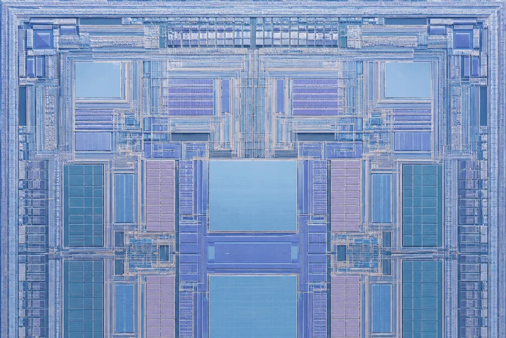
Huawei semiconductor specialist He Tingbo presented new measurements based on the Kirin 2026 SoC. This data confirms the company's Tau scaling law and directly refutes the claim that three-dimensional logic stacking inevitably leads to overheating. This article was published on ChinaXiv following previous versions presented in May and July.
The work emphasizes that heat is the 'most pressing issue' in the context of Tau scaling, but the Kirin silicon samples demonstrate the opposite trend. According to media summaries, transistor density increased by approximately 55%, reaching 238 million transistors per square millimeter compared to the previous Kirin generation, which had about 155 million.
With comparable performance, power consumption decreased: NPU power dropped by approximately 66%, GPU power by 58%, and CPU core power consumption by 41%. Specifically, for NPU, Kirin 2026 provided 29 TOPS of AI computing power while reducing clock frequency by 63% and lowering voltage from 0.85 V to 0.55 V, resulting in a power density drop of approximately 73%. At maximum load, the stacked NPU can reach 70 TOPS, more than double the baseline comparison figures.
The GPU was able to maintain a frequency of 61 frames per second while reducing the voltage by approximately 200 mV. The architectural solution underlying these improvements is LogicFolding—a process of stacking planar logic into layers using hybrid bonding, which allows replacing long horizontal conductors with short vertical connections. Huawei asserts that this reduces routing complexity and resistive-capacitive data transmission costs because, according to the authors, a significant portion of the chip's power is consumed by interconnect energy, not just arithmetic operations. One metric shows a reduction in clock buffers from approximately 43,600 to 19,000.
Kirin 2026 specifies a bonding pitch of 1.5 micrometers with 50 million vertical connections on a mature technology node, with plans to further narrow the pitch in subsequent Kirin models. However, the improvements are not uniformly distributed across all blocks. An early version of the DSP, implemented in a complex architecture, reduced power consumption by 25% but increased power density by 24% due to a 40% area reduction; He notes that a later DSP development for Kirin 2027 reduces power consumption by 47% at a density below the planar base level.
Improvements in CPU blocks are less pronounced because sequential workloads cannot utilize voltage headroom as easily through parallelization as NPU or GPU blocks. He stresses that Tau is a law of temporal scaling, not an automatic advantage in energy efficiency: if developers use temporal headroom only to increase frequency, chips may consume more energy. Future work includes refining the hybrid bonding pitch, combating wafer warping, nanometer alignment, and developing EDA that jointly models thermal, voltage, and layout parameters. Essentially, this story is about silicon architecture, not a new phone release, as the measured density and power consumption on the production-intended Kirin silicon serve as proof that topological folding can provide post-Moore performance headroom without waiting for a new lithography stage.