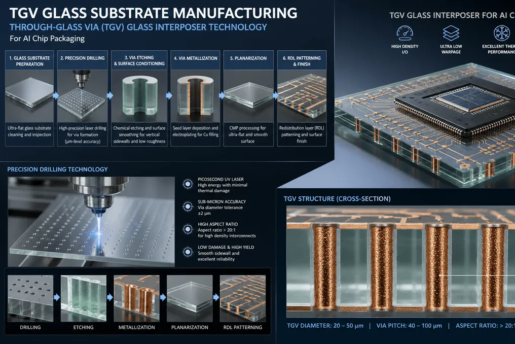
The glass substrate industry with Through-Glass Via (TGV) technology in China is experiencing rapid growth as numerous domestic manufacturers accelerate capacity expansion for artificial intelligence chip packaging substrates.
Advantages of Glass Substrates
TGV technology, which allows for the creation of vertical electrical connections directly through glass plates, is becoming a key innovative solution for next-generation AI accelerator and high-performance computing chip substrates. Unlike traditional organic substrates and silicon interposers, glass substrates offer superior dimensional stability, higher routing density, better signal integrity at high frequencies, and thermal properties that better match silicon dies, reducing warping and increasing yield for large chiplet architectures.
Demand Driven by Chiplet Architecture
The paradigm shift in AI chip design towards chiplet-based architectures with high-density interconnects between dies has created an urgent need for packaging substrates capable of supporting the required routing density for inter-die communication at throughput exceeding terabytes per second. TGV substrates can provide finer line pitch and smaller hole diameters compared to organic substrates while exhibiting lower dielectric losses than silicon for high-frequency signals. This technology is particularly crucial for AI accelerators that integrate compute chiplets, HBM memory stacks, and I/O dies on a single interposer or substrate, where routing density requirements have surpassed the capabilities of conventional packaging technologies.
Production Scaling and Supply Chain
Chinese TGV manufacturers are increasing production capacity to serve both domestic AI chip developers and multinational semiconductor firms. Key players in the glass substrate ecosystem have announced expansions in capacity for glass base substrates and glass interposers with the goal of achieving production volumes by 2027. The supply chain for this technology includes specialized glass compositions for semiconductor applications, hole formation via laser deep etching or focused electrical discharge, metallization for reliable electrical connections, and final planarization for multilayer stacking. Chinese equipment manufacturers have also developed competitive tools for TGV drilling and metallization, reducing reliance on imported manufacturing equipment.
Market Prospects and Integration
Sector growth is supported by the broader reshoring of semiconductor packaging supply chains and China's ambition to create a complete advanced packaging ecosystem. Industry analysts predict that the TGV substrate market could reach several billion yuan within five years as its application expands from high-end AI accelerators to network chips, RF modules, and MEMS devices. The technology readiness level has advanced from the research stage to qualification for pre-production, and several Chinese manufacturers are now capable of supplying TGV substrates for AI chip packaging. Vertical integration of glass substrate supply within China reduces the exposure of AI chip developers to cross-border restrictions on advanced packaging materials.