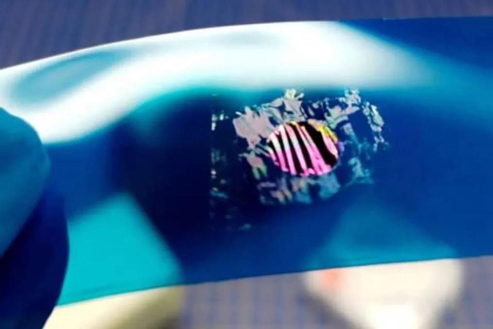
Researchers from the University of Southampton and the National University of Singapore have presented a method for creating two-dimensional heterostructures without using polymers, which are traditionally employed in this process. The results of this study were published in the journal Nature Communications.
Replacing Synthetic Materials
The proposed approach replaces adhesive synthetic materials with natural muscovite crystals, which is a type of mica. This allows for a reduction in microscopic contamination that typically degrades the quality of structures composed of layers only a few atoms thick.
Potential for Quantum Technology
This achievement has the potential to increase the accuracy of research using quantum materials and accelerate the development of more reliable electronic components. Surface purity is recognized as a critical factor for the performance of such devices.
Overcoming Nanotechnology Hurdles
The production of two-dimensional materials depends on stacking extremely thin atomic layers. Standard methods for this assembly use synthetic polymers, which leave microscopic residues that alter the electronic behavior of the structures. To overcome this problem, the team used muscovite, a mineral known as mica.
According to the researchers, because muscovite is an inorganic crystal, it provides a more uniform surface and significantly reduces contaminants during the assembly of heterostructures. The work also demonstrated that this substitution allows for the placement of atomic layers with greater precision. Such control is important because some two-dimensional materials acquire completely different properties when stacked at specific angles.
Significance of Precision in Quantum Research
The study's lead author, Marcus Shishkin, a professor of experimental physics at the University of Southampton, emphasized that this level of precision is critical for research in quantum materials. He stated that when two-dimensional materials, such as graphene and hexagonal boron nitride, are stacked into structures with controlled angles between layers, they begin to exhibit entirely new properties.
The researcher explained that small amounts of contamination can distort experimental results, so a cleaner process expands the scope of scientific inquiry. He also noted that the new method simplifies the fabrication of structures and reduces process costs.
Prospects for Nanoelectronics
In Shishkin's assessment, improving contamination-free fabrication methods is an important step toward creating more efficient nanoelectronic components and, in the future, faster and more reliable microchips.
Alexey Berdyugin, a professor at the National University of Singapore and co-author of the study, noted that creating atom stacks without impurities remains one of the biggest challenges in nanotechnology. He added that since mica is an inorganic crystal rather than a soft polymer, it avoids many contamination issues inherent in traditional methods.
According to Berdyugin, this method provides ultra-pure surfaces, allowing electronic components to operate at maximum performance. The researcher believes this feature could pave the way for both fundamental research and future applications of quantum technologies.