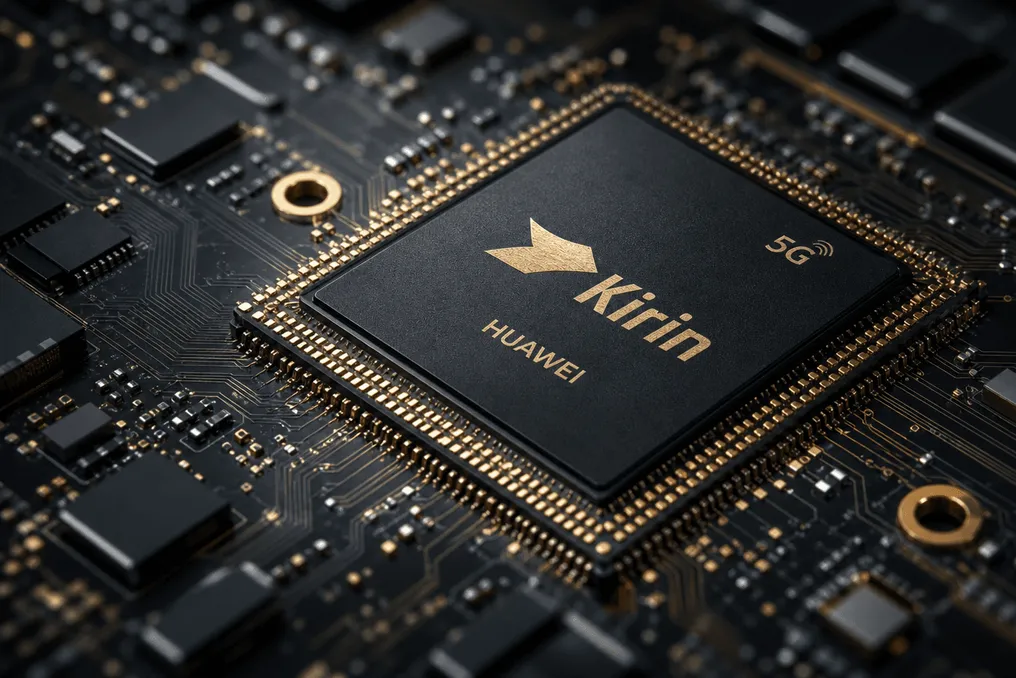
Huawei has released the second version of its scientific paper 'Tao's Law,' titled 'A Time Scaling Theory for Multi-Layer Electronic Systems.' This document demonstrates the company's systematic approach to maintaining chip performance scaling in the post-Moore era, despite limitations related to the embargo on advanced EUV and DUV lithography equipment.
The Principle of Tao's Law
The concept of Tao's Law is named after Huawei semiconductor business president He Tingbo. It is based on a complex time constant function $\tau = f(\tau_{transistor}, \tau_{circuit}, \tau_{chip}, \tau_{system})$, which divides system time into four interconnected sub-constants at the transistor, circuit, chip, and system levels. Engineers achieve full scaling of the $\tau$-function by compressing delays at each of these levels.
Kirin 2026 Innovation
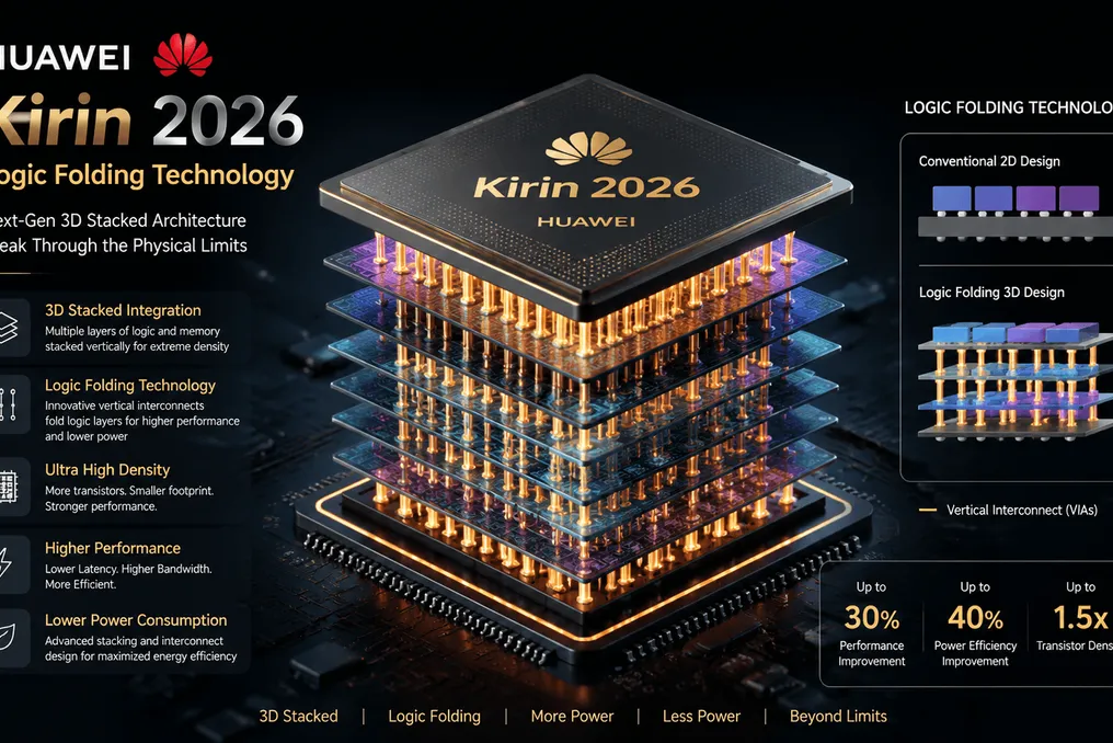
The Kirin 2026 chip, which will be used in Huawei's flagship smartphones of 2026, is the first mass-produced mobile SoC to confirm the applicability of Tao's Law. Its key innovation is the 'Logic Folding' design methodology. This method distributes registers and logic circuits across two layers (wafers) connected by vertical hybrid bonding interconnects. Unlike vertical stacking of DRAM in HBM, Logic Folding separates functional logic components across multiple die layers to optimize hierarchical layout.
Advantages of Logic Folding
This method can be compared to converting a single-story house into a two-story duplex without changing building materials. By not relying on more advanced lithography or smaller transistor sizes, Logic Folding reduces long metal traces on the chip to short vertical channels between layers. At the circuit level ($\tau_{circuit}$), this ensures the miniaturization of the time constant.
Performance Metrics
When compared to the baseline Kirin 9030 Pro model, manufactured using identical processes, Kirin 2026, equipped with Logic Folding, achieves a transistor density of 238 MTr/mm² according to Huawei's measurement methodology, which is equivalent to 175.39 MTr/mm² by industry standard (excluding auxiliary isolation and filling devices). This represents a one-cycle density improvement that would traditionally require three years of geometric scaling. This density slightly exceeds the logical density range of the 5 nm planar process from TSMC, which is 138.2–171.3 MTr/mm².
Energy Efficiency and Forecasts
Furthermore, Kirin 2026 reduces the supply voltage by 0.2V while maintaining performance equivalent to Kirin 9030 Pro. The measured power consumption is only 59% of the baseline level, and the power density is 94.4%. Huawei emphasizes that Kirin 2026 uses a conservative implementation of Logic Folding, indicating significant potential for further density increases. The company forecasts achieving a transistor density of 400 MTr/mm² (or 294.8 MTr/mm² by industry standard) or higher by 2035, with Logic Folding enabling Kirin core frequencies to exceed 4 GHz.
Application in Data Centers
Tao's Law is also applicable to artificial intelligence applications in data centers, where over 80% of energy is consumed by data transmission and over 70% of system cost is attributed to data storage. Huawei's implementation for data centers includes a Unified Bus architecture, a Hi-ONE near-package optical engine, and a 3D Folding packaging topology to compress communication time constants at the $\tau_{system}$ level.