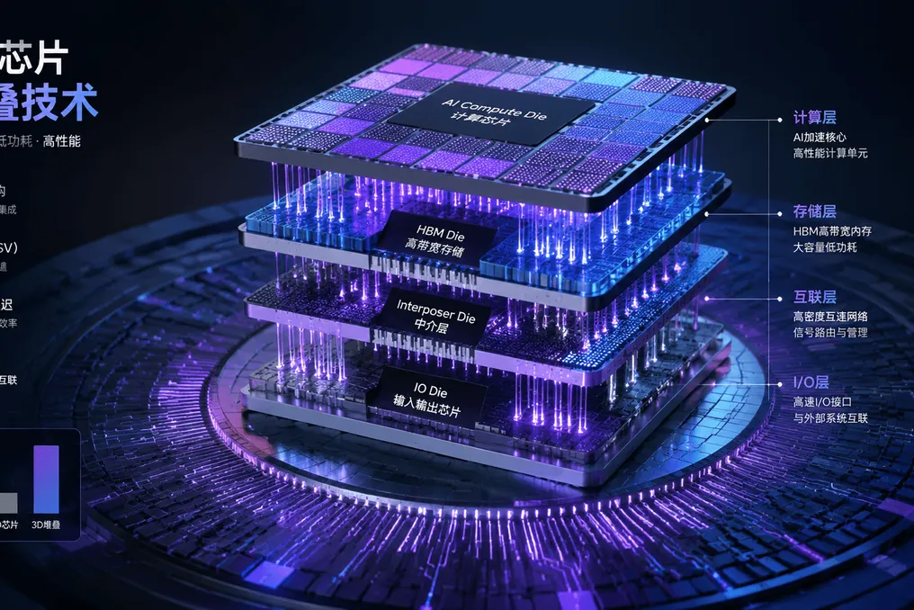
Chinese companies producing AI chips are increasingly utilizing 3D stacking technology as a strategic alternative to upgrading advanced process nodes. This is happening amid the industry's confrontation with the physical limits of scaling flat chips and restricted access to cutting-edge manufacturing due to US export controls.
Overcoming Memory Constraints
The so-called 'memory wall,' which arises when memory bandwidth and capacity fail to keep pace with the exponential growth of AI model parameters, has forced the industry beyond the capabilities of standard 2.5D packaging technologies like TSMC's CoWoS. These flat solutions face fundamental limitations in resource routing, integration density, and reducing chip area for high-performance AI workloads.
Application of 3D Stacking in China
Several Chinese chipmakers are actively implementing 3D stacking solutions to gain a competitive edge. The company Tsingway is developing next-generation AI chips using heterogeneous 3.5D stacking. This architecture combines reconfigurable compute chiplets with vertically stacked DRAM in a 'four computing lanes plus four storage layers' spatial structure, significantly boosting data throughput and computational density.
Suanmiao Technology introduced its A4E TokenPU chip, which features eight layers of storage die vertically stacked above the compute logic. Thanks to TSV and micro-bump interconnects, this chip achieves a memory bandwidth of 16 TB/s. Lingchuan Technology, spun off from Kuaishou, developed a chip with fully domestic 3D stacking technology and an innovative 3D memory architecture adjacent to the processor. This chip is based on the SL200 model, which has already been sold to about 100,000 units to companies such as Alibaba Cloud, Baidu Cloud, and Bilibili.
Other Developments and Challenges
Unisplendour's Zixuan architecture focuses on 3D-DRAM with a target memory bandwidth of 30 TB/s and a Processing-in-Memory (PNM) mode. Meanwhile, Intellifusion is developing inference chips with 3D-stacked memory to ensure higher throughput and reduced access latency. Despite serious challenges remaining—including thermal management for stacked dies exceeding 350W, which requires liquid cooling, improving hybrid bonding yield, and the limitation of domestic EDA tools for 3D designs—the adoption of 3D stacking marks a strategic shift for Chinese semiconductor firms. This paves the way for increased computational performance regardless of the progress of the process node under conditions of limited access to advanced manufacturing technologies.